Kanwar,
Thank you for your response.
I am not upset, I don't even have a temper.
I have a question, if you wouldn't mind?
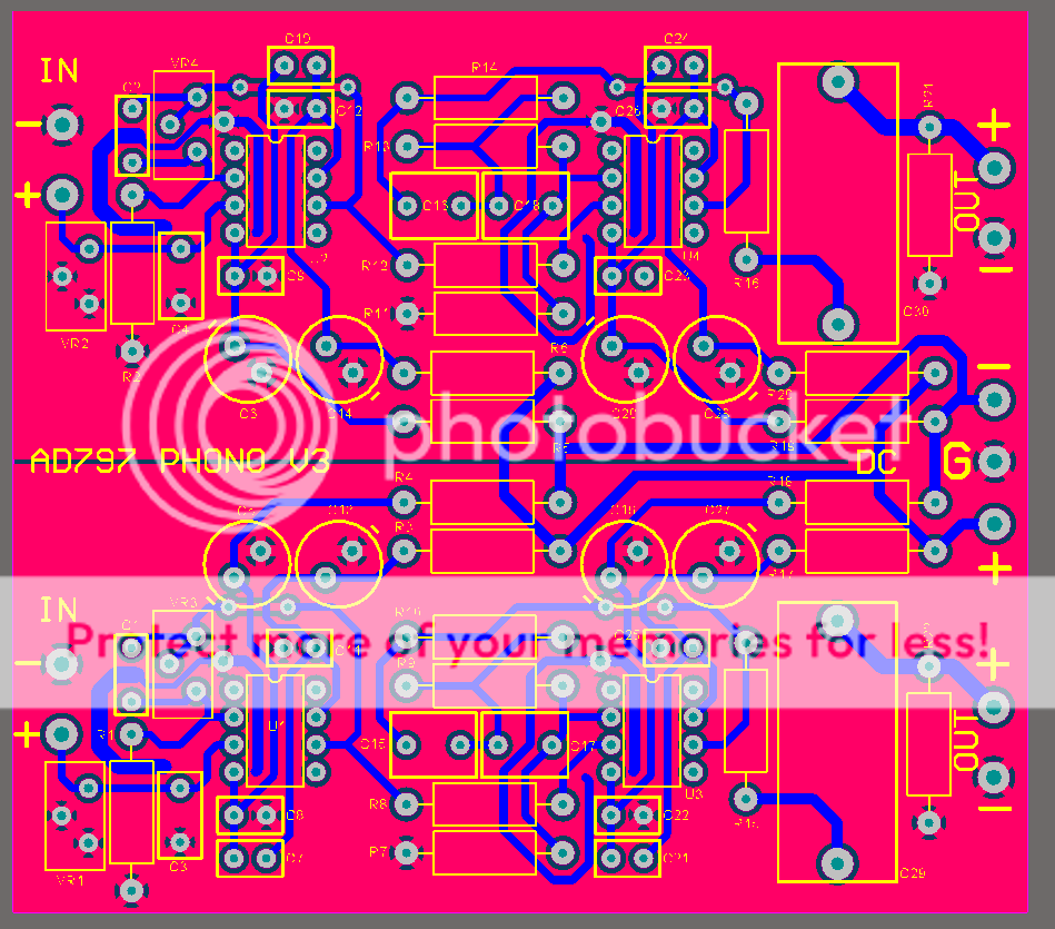
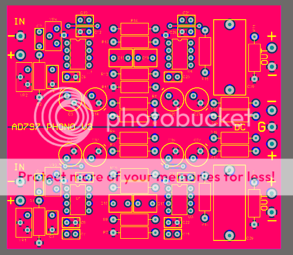
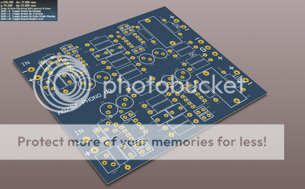
If using a double sided PCB with an uninterrupted ground plane on the top how do you suggest routing the supply rails on the bottom without crossing other traces?
If you can show me the schematic, i can make a conceptual layout for you, which will include the said power supply tracks, differential filtering, common mode filtering as well. Along with the tips to create a guard rail surrounding input nodes of the opamp, to keep the RF out of picture. Also i need to see if you are using the recommendations given by Scott Wurcer the chip designer himself about the stability criterion.
Since you use batteries, lot of contamination is ignored just due to pure DC source which in your case is a big helper in this. Otherwise if you try to use other types of power supply source , many things will come up.
Kanwar, You are Guru. Please help all small time DIY'ers (here in HFV) with some constructive suggestion (of-course using your knowledge
")
). This could lead improvement in said project and some enlightenment to us.
Mishra ji,
I am not guru, i am still a learner, i always love to help people in correcting mistakes in diying as per my knowledge capacity. There is a term constructive criticism, if you look at my previous post you will see that when ever i pointed out mistakes, i also gave the reasons behind it and correcting ways along with it.
There are certainly exception where you want to cut ground planes and separate them to avoid unwanted interaction between PS and signal. Also PCB ground lines sometime needs Star grounding which conducts ground currents from parts to Central point near PS. Also ground plane and surrounding copper which is not in path of return current still grounded and separated for shielding signal and its return path. Isn't that so?
Groundplanes are cut into small islands and then grouped/clubbed into a STAR ground whenever you have different set of circuits such as digital and analog sections present on single PCB, such as in DAC. But in this case also, the ground planes are not CUT just to route power supply rails. Although small jumpers are permissible when necessary.
If you look at multi layer boards, there you will see Top layer being groundplane, then comes 1st mid signal layer and 2nd mid layer being a power plane which is nothing but a power supply rail having properties of a ground plane. The idea behind this is to keep the potential especially the common mode component confined to minimum and keep the inductance to bare minimum.
When you use a grounplane it becomes obivius that certain return currents are always there, for example if the decoupling capacitors have one leg joined with groundplane itself.
Here is an interesting article regarding right angle traces:
Who's Afraid of the Big Bad Bend? by Dr. Howard Johnson.
Who's Afraid of the Big Bad Bend?
I would like to ask Mr. Howard a question about the ringing and delay in settling time on squarewaves when driven through right angled bend vs octagonal bends.

Ringing is directly proportional to the EMI ingress and RF contamination To and Fro.
Numerous experiments are done to validate the effect, i am not alone, but great names in instrumentation engineering have numerous white papers on high speed PCB design with an indepth analysis on this subject.