In india, a DIY enthusiast faces one common problem that is to get the PCB done.
There are lot of firms that manufacture PCB but the ordered quantity required is very high else order value should be minimum 5 to 6k .
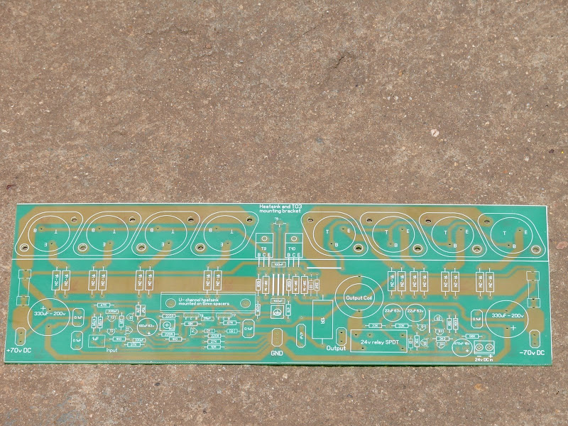
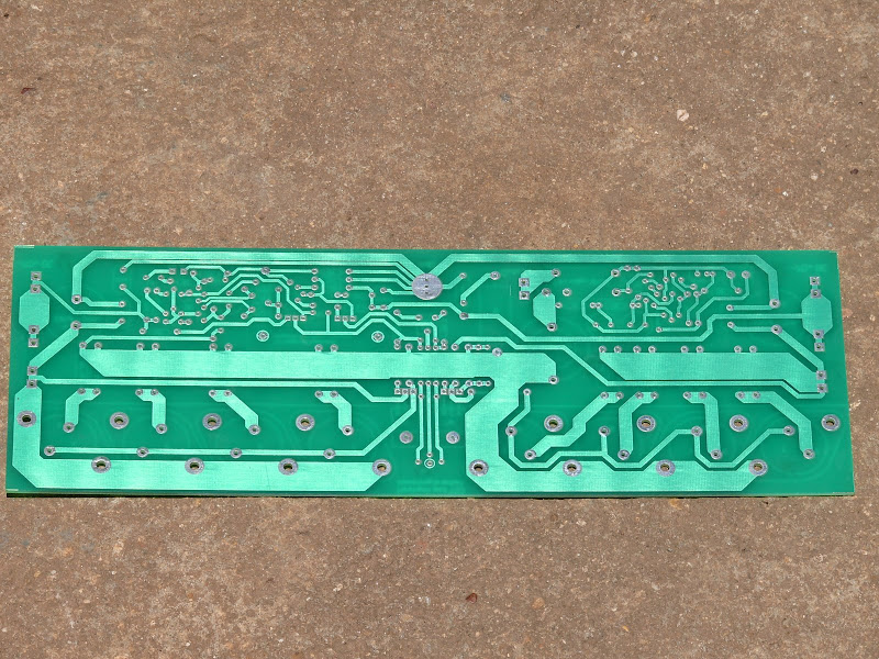
This poses a big problem and also ordering 100/200 pcs of pcb for a experimental project is meaningless. Here I present a guide that will help to fabricate PCBs in quantities of 1-2 pcs at home .
.
~IRON-ON PCB FABRICATION~
It is based on the fact:
"Laser printers and photocopiers use plastic toner, not ink, to draw images. Toner is the black powder that ends up on your clothes and desk when replacing the printer cartridge. Being plastics, toner is resistant to etching solutions used for making PCBs - if only you could get it on copper!"
Source : Documento senza titolo
Material :
plain copper clad board : mostly available in cities
Photo glossy paper : used for printing greetings ,invites .available at stationary shops
[5/- Rs a sheet approx]
laser printer : to print the layout
PCB design software : Eagle [free version]
or Express Pcb or Free PCB
One cloth Iron
Steel wool: availableas utensil cleaner ,Kitchen scrubs
A hand drill for PCB drilling .
Chemicals: Ferric chloride [for etching],
HCL[optional - just as accelerator] -usually the acid is available as bathroom cleaner
Soap , plastic tray/bucket
The text here is a quick summery of the procedure .
> Design :Use PCB Design Software :
alternatives are
Eagle free: has some limitation as per component count
Express PCB :Free easy to use, i preferred to use this one !
it will alow you to print the layout , Use a virtual PDF printer like
pdf 995 . get the pdf , you can take the same to the neighboring printing
shop where you can get a laser print .
Note that it may add some dots in the final print , these can be later scratched out from the board.
>Printing: the design should be printed on the photo glossy paper ,try many types to choose the most suitable one.
> Board cleaning: never touch the board copper side ! ....first scratch the copper sid ewith steel wool till it gets clean and shiny
>Iron on: Important : place the the glossy paper where you printed the design over the copper side, so that it doesn't move,u can use clips.
heat the iron at max setting , Iron over the paper side 3-4 time , press hard doing so.
>Remove :As the paper sticks to the board , let it cool ,put in water ,let it absorb water .now slowly rub the paper and the paper goes away leaving the tracks
>Etch the till you get your PCB:
Now take 20/30 g ferric chloride mix with water just enough to dip the board on the plastic tray.
place the board on the mixture and leave it for 8 /9 hours apporx.
if you have the diluted HCL add it a little , this will accelerate the task and will take 4 hours approx .
After etching remove the black ink by scratching with steel wool etc. Your board is ready now !.
!.
Use the hand drill to make the holes , this is a tedious task as one has to drill 70-300 holes depending upon the board !!
In case you stay at a place where you cant get the materials
you can use the PCB making kit is being sold by vegakit[do a google] .
There are lot of firms that manufacture PCB but the ordered quantity required is very high else order value should be minimum 5 to 6k .
This poses a big problem and also ordering 100/200 pcs of pcb for a experimental project is meaningless. Here I present a guide that will help to fabricate PCBs in quantities of 1-2 pcs at home
. ~IRON-ON PCB FABRICATION~
It is based on the fact:
"Laser printers and photocopiers use plastic toner, not ink, to draw images. Toner is the black powder that ends up on your clothes and desk when replacing the printer cartridge. Being plastics, toner is resistant to etching solutions used for making PCBs - if only you could get it on copper!"
Source : Documento senza titolo
Material :
plain copper clad board : mostly available in cities
Photo glossy paper : used for printing greetings ,invites .available at stationary shops
[5/- Rs a sheet approx]
laser printer : to print the layout
PCB design software : Eagle [free version]
or Express Pcb or Free PCB
One cloth Iron
Steel wool: availableas utensil cleaner ,Kitchen scrubs
A hand drill for PCB drilling .
Chemicals: Ferric chloride [for etching],
HCL[optional - just as accelerator] -usually the acid is available as bathroom cleaner
Soap , plastic tray/bucket
The text here is a quick summery of the procedure .
> Design :Use PCB Design Software :
alternatives are
Eagle free: has some limitation as per component count
Express PCB :Free easy to use, i preferred to use this one !
it will alow you to print the layout , Use a virtual PDF printer like
pdf 995 . get the pdf , you can take the same to the neighboring printing
shop where you can get a laser print .
Note that it may add some dots in the final print , these can be later scratched out from the board.
>Printing: the design should be printed on the photo glossy paper ,try many types to choose the most suitable one.
> Board cleaning: never touch the board copper side ! ....first scratch the copper sid ewith steel wool till it gets clean and shiny
>Iron on: Important : place the the glossy paper where you printed the design over the copper side, so that it doesn't move,u can use clips.
heat the iron at max setting , Iron over the paper side 3-4 time , press hard doing so.
>Remove :As the paper sticks to the board , let it cool ,put in water ,let it absorb water .now slowly rub the paper and the paper goes away leaving the tracks
>Etch the till you get your PCB:
Now take 20/30 g ferric chloride mix with water just enough to dip the board on the plastic tray.
place the board on the mixture and leave it for 8 /9 hours apporx.
if you have the diluted HCL add it a little , this will accelerate the task and will take 4 hours approx .
After etching remove the black ink by scratching with steel wool etc. Your board is ready now
!. Use the hand drill to make the holes , this is a tedious task as one has to drill 70-300 holes depending upon the board !!
In case you stay at a place where you cant get the materials
you can use the PCB making kit is being sold by vegakit[do a google] .
") . For more dense PCB just 1 to 2 pieces one can order at PCB Power - which is an indian mfr.
. For more dense PCB just 1 to 2 pieces one can order at PCB Power - which is an indian mfr. !! he's a spammer and has posted a Spam !!
 !!
!!
