Can Some One Verify my PCB with the Schematic

sadik

Well-Known Member
Joined
Jun 14, 2015
Messages
1,035
Points
113
Location
Vadodara
Hi Friends,

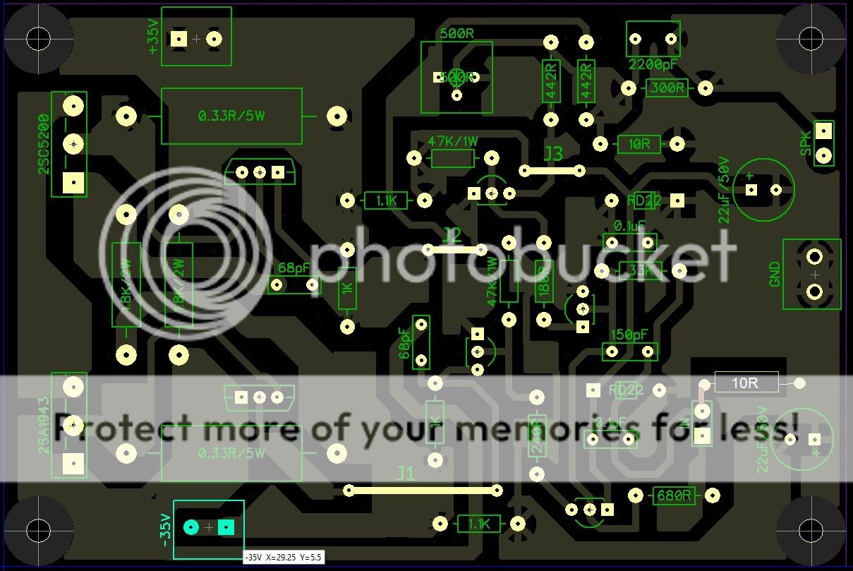
I have made my 2nd PCB (Jean Hiraga 30 Watt) in Dip Trace(Demo Version) I would like to request the Gurus to have a look on it and verify it.

If there is some mistake please download the Pics and point out the mistakes by editing the Photos in Paint. please accept my apologies for same because I am not an Electronic Engineer nor do i have that much of knowledge to understand the mistakes just by reading.

I Would specially request to verify the Pins of transistors. Below are the Pics of schematic and pcb.
EshtFI8e9KdcmI2S0XnVlnStXmKktJ9dposuLwqlaKembkzzXcdyAzw81UR-_EdywpO2LEVVSiB3G5xTmaphopoe4pERwqYLouF6dM896kP9E2hrb_lwhRmsVf16uGRthxjUNZFIRVPXZMSmDBQIHVwdSazhyHcSA2JYXsgn0dFEy9JiIW8bqrk7bE67M0gRmdSKo0gggUZV-LzDeDvv3BMXNARJnTj_kzWJQPzv9EK3FMAvHokHGRm0WgKPz-w5DOUljCriJ379fEB8W_U8GPRpYL5qTmsR7nd9KQBYJP90TTmZ7liIUbyaukwEhjNMUlUrl2kQLz8nrfbqX8L4rt6DIbGfOsRN6cfJeC6KE7o-F93tXL_icpgtg9D22IQ2bpOc7wFO0SGf-zziHQxvqxBM8apNvdGnIEX8JxvyQr56YDUcsYfePzV2ilCFFG6yRuI-UMCmbFZOBFbIqBxk0kc4jlb5Ump2DCUJ0MhNPRFA4dMwicLm1T_dz7LNwBy5wI4YLMn0-_CNsi195_3mDuCZqj1wtNyMhkhDvAGA8JmDdLe07Xj-64HoBGIft2NkBlh1CpW2MW-CYQagGnCQDAXVxpdPEBM=w1898-h922-no

i47jVsVY_zSLJ2RaqFzWnqxW0Xc4v8l6GMFZOAQCPFoAmlyTfJJz93jcXJrMTw85fej1ix7EklPqmogbarSjAvHJ0qXTTJUS4RVfxzg69SaIBFVsUwDfWNAuDhi-IHC4zJzACV86Gsy73gXejzUvDJrW1ZwFbMFz5Jw_cuzkWxhzHFM_-GDsic72cmyXHxrgrCPfKXiJ3gx0sDwa1oUHiW0GggO8Jsgmp9-8po0Nkn_-fDkYK1RzIUkY8IBu11xv1_yMg4giSgDVFrWlpNJN58Rbyh_j89Gydvzg2XkmlQnYcWeOoPjc9kAImEYfHmBSI7TnwH9ZxFMvctyMhfBUGdEOBG1NJmL53_AoQamjQZe-1fq3jI7aXPIZb7FpQp4KLJjmD6JgxMxdTjOguyjRnzqteOeL16NEj32NcfruV3XYFpd6jKvhNs7oZwclwb2SKIFbL7RcKwJOfxbjdVBmQDd7-Rw6s-t2IWSUxRjmJcUkyQwqDHl9_oyz8DAmpHKUPjRB9h6xsakoBWV3YEe6kNsP61t0hb6AoE0uSeqonUhhCe9WjdDndBLtkEff8UOzYXoP1m36JxaDKA_zJ2XR85l8_WPKR7Q=w1121-h857-no

Regards,
Sadik
 
Hi Sadik,


Is the schematic correct?
PCB could be improved a lot more. Good effort though for a start.


Regards,
Aniket
 
Below is the original schematic.
khv3p0goMD_htxlshj36AjvDVpTIYQ9dwhlWAV3uLfHNdDBnbwck33v13A_lMTIqp8EiwC5NhNY7yrs3w3jiwJ297_Gf09y4NZcl3oMJ0ogKLar5OUH5-f2USKATMmYIvD1qffrFMFxMr_zruksXHSLcFoSjuKvzIJWNuaeVtSReaJMWTBa-iOAMStiOoD_dqUNer2bCYaDwnWS0xmvOU9V1pg_XdEGkhbuzwqG5Ya-KsgZb0lQfWcyplVVAPbh7WAMcwLy55plkGONCWSShw5XC7CdbEm5mqhTYvsVJw5wB1GVqr7ua1JjpoBS4Getg7O-eUAI27NzuQC00UAUP4IPDjaAjGXprVA50iyyu8YOz8I3NPn-15Jhd8_kCRSYthQJ6d_z_o5J4KxhDSn98rP6SVPBEP49j0wQDEMFKiHDA1LWklUKL4UiqGevoKRZ3Li2LwtP_KtBliLp1Y6v5Z5XxVCghfcfwTBRh6WARneRzHxFVAd1HgrOTbvL2SGmaOD7MRegmrze1AtVUb8lQgIhm1rX3KKw2iJbDR4nVZK-r3rulqrTcwFBtjhKg45P-dJUpi7ECLOHm4jj_TFUNpY-xLfwziOw=w650-h600-no


I have replaced 2sa872a & 2sc1775a with BC547B & BC557B

Sadik.
 
2SC1775A/2SA872A and BC547/557 are not interchangeable, direct replacement could be 2SC1845/A992 but are hard to find. 2N5551/5401 could work as well and are easy to get.
2SC1096/A634 are also extinct, BD139/140 could be the replacement.

there are a few errors on the PCB, few things to consider:
1. short and thick power traces.
2. input circuitry to be kept away from high current traces.
3. thick traces for ground.
4. signal ground to be separated from other grounds and should go directly to star ground on PCB.

if you could get hands on some better PCB design software, try Eagle PCB and Sprint layout, both simple and easy to DIY.

good work Sadik:)


Regards,
Aniket
 
Thanks a lot Aniket i'll redesign it. I Didnt understand the 4th Point though Can you clarify it in detail just by uploading some kind of Figure so that a learner like me can understand.

Sadik
 
Thanks a lot Aniket i'll redesign it. I Didnt understand the 4th Point though Can you clarify it in detail just by uploading some kind of Figure so that a learner like me can understand.

Sadik

I mean to say, the signal ground i.e the ground which is connected to the audio input of the amplifier should be a separate trace and should go directly to the ground connection on the PCB.

In your PCB this ground is shared by rail filtering caps, 22uF, 0.1uF, which should not be done. use separate ground connections for rail filtering, audio signal and speaker ground. ideally speaker ground should be connected to the power supply ground.

Regards,
Aniket
 
Hi Aniket,

I Have redesign the PCB & shifted the Power tracks on one side & signal tracks on other, below is the Photo. I Still did not get about the Ground. Do you mean to say that the Ground for Speaker Out should be taken directly from the Power Supply Ground?

Hf7wXrcN2uCq0O3e5Mq3XV2YrmF8dnNvj3IGeirMPIoyvL98jkqAU5uylndGbfHwg9k9-aZF6CQ91EABN2OemaLnsPSIcd4hqfWRktCn8XaUYkSZQ4EeXsWbg3FW7bWAxTxjVyvSMskWs19i4s2cT_U7MWSNsJk4ri4muEheEEjThEbgzNidCw-qYnrDRK883ivE1uztz6sbjYL2iHslErNXitk9ENQYFku5Uavl6U8Sxsac6ykRj-jElEeIrv3X_hvcCbAzn-Qz8gOx5Cx19GWgGYPCQ9gQqzgEpca6OxaWg_79tkTbeHBz1dVN0McVYgsKt5iu6ZPIafxwqz8W-tmqilSoBInejLSgDSNTHAN80QpIgbZK0atRa3CTK6unO6hxZTa3V8FUwm_LsErI0wymSd3lFUmoAlCR9IrZ0vMvYC2eJIdQ4N37UkK4Jn-I_lSk4HBLDB3lY2DGnJOzY1cDKSLaY71AzhKVqxXJA-PFKxbZAaT2EbMH0FpUWcydEWudkn3A7zpXVKV3y1gzDGwKG1mt9UBVOE4RlQvYs7H7sxWhXB8FUlBeo4QUWj4mhgtVbq5qRR1fJm-YxZ16xd5SinZs7wk=w1201-h801-no
 
Hi Aniket.
From what i have understand i have made a wiring diagram. Do have a look on it.
V_S6ztEtytyz04sBOV8l-H2MkuctgIJLfw0M8rPTFxUGorLEXBwAdsi2R55PQsRlNh1xb-osOxdSp2vKLdM5wluJRJdWWjEVZeO-2XjF8EQ32tXxT7d0su6Y7xAmXUGbkJEUvi86X61_Hp_pesC5i-mHWE09gCLRsfdpPydO-7-fz-XihPHoit77bvrWkPFwYqot4WDqeZUT_ZqR3GJfayZsoGtu4Ik-kSH53Ff72D1N4vo8OEnOlfnkNw5e9_MeGJCtzkGMrFqvrjqxGi6osHTpptuqYcxQWFaJlCwBcNYGnEqyiVS8vXTTQEfM3AkKJYMAxUTUbFRr6f5QChrpO315VeUlfZ-djF7GW1cV6aZVf1xZbxTJwx3qDro-rUIkCJnWAjSCOzEEK5Lgdyf8mURiWTgx_UxvIzyYrmztQJ_UP94I1k6UDyKsU1OBAAQXJbkJl_pYqdf1vqbLIRf6_u2OgqYp_WnFcKMCdr0d0T9DUpw2ROXlZsWtmHLAeVDLiVaCoYLqRzDy1EXeWgAIiZ0wspkQ65tD5VeNlYe5z8LsQYXAkKL6StUyRWmHigOYGeM3B-f0oUFw4hdL2MwAPYT4D0mMqDo=w905-h745-no


Regards,
Sadik
 
JH%20Wiring_zpsvbjrlg9v.jpg~original
[/URL][/IMG]

It should be done like this.

there are still mistakes on the PCB. try out sprint layout, much better to DIY.

Regards,
Aniket
 
HI Aniket,

Thanks for the wiring layout. Now i did understood a bit more. Based on this wiring diagram i modified the PCB. Now the GND and Signal GND is seperated.

Regarding Sprint layout I don't have any Idea. Dip Trace is familiar to me and is very easy to operate also.

Below is the Photo of New PCB based on your inputs.
jZ5Xf-xRkpCivIlGdnfLB3F2q_fpTGdkvayM-Bv1N3Xc7RdDw_SfILEFgY3T3dhPAsnUwRGK7wO-KorEQu_QZ7c6ExSgO1qi1fHQJCiAv3ONK3_v4xomEiVSjTZDawTeLzhNvAUK-aOi-JRq2lX0Om3DZNFp1P6IErZschR0QqXt4Lr5vywe7Oskky9wuidaEAKx2XWEEaqs8_3k4kax2MAnBLzVnCfdRx8MW1L2Gm4xuDvxwD7R7g7pPJnA4z-pYU0iOQnl8Oh-VZuxkcY7v_MeGIrXfNVVxxQHJOkorB6q8xxhF3vvoYXp3HdsuV6ZC0m0WDTN5i6jV6XHtFan3jPzuXkf_4tGwg_ieKAf--lLDSLrIAUhux6XwDUk2tbT_rGkfNgswZ2an4KAo8YZn0eLOk0jUYP8GqVo7fvUtCa8vFC149mMTiY52BWyvqbp6wcgCsza-z5wHU4PfDzGu48omJa_xSLFVwjiRizuZTk6kMTyOtFWQfzRwy7jnmH7lWoLnE2zBUYD3mQnok9JwG9-YQY3Qqe3bZmO5WtgmHlteo-SaK7Ei3EsUUh6w_TwP0zD11DycA2iUneZ-AkBODP5Q_4Eu7U=w1209-h809-no


Once again i thank you for your help.

Regards,
Sadik
 
Hello Sadik,

1.you have separated GND and signal GND, but they should be connected on the PCB itself. there are still some errors on the PCB. Since you are using a ground plane you could have connected the signal ground to the ground. no harm in doing that.

2.speaker connection goes nowhere, it should be connected to the emitters of output transistors. look at the original schematic for laying out components and traces.

3.sprint layout is even simpler than dip trace. still use what you are familiar with.

Regards,
Aniket
 
Thank you once again Aniket. That was the Major mistake which you pointed out. Now I have done the Correction, Tere were some Pins of Transisters which were interchanged & same is also been rectified.

Here comes the Final outcome.
muQQ7UDLQVAMUbY2NcK4HQmbzCD-T9sslKrjZErmLpP2rIdxIMYW1vZm5m8_D7KanL4MKJslAyjGWR2ZDKMvck9HgjQ_1Gx6AdcNFLd3KnozS2swq6C7L-S87rk4ozMJ9Lh1qoRRzkIhq9e7ov_7y6I2dkIqGilS2ebOJ44YOvapfgwi2R8GiXZAHc0JZetcr1Te5Fg-YWcTQz6zeoEBa97bOngpX-ivAS_pMir0XRsUE2Br0x97sGugsVGcpWq6aGVTNACGrtFlxq6QH1XbsI4S7ukPNVtk-mm4CvOVKrJ9pYxfxJ-7omFPP-4_EjIaTJelY21ggnrckxPfXOoIOHaDhnNSKEFjkwPazh8c4VLYxzMw4neZM-jdl5SP4ur8haYXGIraay60HtFjnkQFZsDXB-SyAuTKYFb0D0DlP1z-8vXo7p67TAgMO9w77omUqK9m_lmuy0n8VQ9XoFhs1BWZGFRafeSqpQPJveFp4atn7mzZMWE8cx5y47WcKik74LEcUI_HnuuMd_WHCCRY7lGAHWRpZ2nDiOnvXUC8BMNbkB7hOoFzhv-n5pWjRBP0ARqA6RuUQoJ-kJ_8RALT5HcmmQJmGjakoHA2Kw6aKfBEKAUd=w1120-h750-no


Regards,
Sadik
 
Good work Sadik,

actually PCB could be improved a lot more. but great effort for a start. are you going to etch your own or get these made from a manufacturer?
 
Good work Sadik,

actually PCB could be improved a lot more. but great effort for a start. are you going to etch your own or get these made from a manufacturer?

Already itching & Tinning is Completed for Single PCB. I will assemble this board for R&D if there are errors i will resolve them & when it works well then i will make a pair.

Below are the Pics of Itching, Tinning & Silk
Itching
sApqJRimcoSMri2UTYXfPwnV83zLrE38iJDpMMs_ZrigUwI4fdfeqXe38l7kq43mWNS3yU3tPlPKByXtN4biRUXdrSjylocC0NEfeolp9ZPQQ0UG9bVV_OSQc7UICfzUqdTQSOvg1GLoo7A5QZh8ffaPDBqEFwFiNgLMpbwEyMHOwpnePNyybq-xVGYh3PebEYA2z25o6ghPQSdSBF-k9JPm67E8LhwDTLydMNuWWaIC70zpjShYaYmE5rR1AtKUcfh7ep0dsyLUrTfeK9P6aq0lWpgzzLDq8UQXQJchsCbSdpdp1sSoxurG0OJvV8F-D5ESvHYZ317iL-jT7Yop1_28DQO5QWtgxInsGTHbiedB5GZ-UpUCOrSpGEniCAJ4Rs9W6pQAYRBDcwlOds0J8MRt0exQGrOIL7N8g1mHQi7NWmCRVKt_Ta2cshveFwzjiqZmzCmvJ6MZNwnyAj0v0cfNXoJkFdeXPzrIbcL3KRPJ0Yjn6RMPDYQ-17Yn1GGn7tISDeUbeMVSYK71Kh9qroBzcrvFHHwfGZcT7rHmvL6XINQoB8tkJGeXbf9Ucf7PAGf1IMwTaQho_vN3XkP7Puz_W8bePeA6M3Jt2InGuqCHS-88=w1230-h922-no


Tinning
4B0_NYKsX78EBPagam56RxxEws67dopGODvFX82c62IMqXkoJC2qMq-pa77kdgIZL8cyNoKe09KOCO94OQ9Qd1FHpvcofxSUWBDMi6jADwGdfq8v8jEV8ac-GCKUVUHcJDrsMBGpxDAERDXvi6IxHf3BwsS2XqWxwMel5F7hV1b4DLYq-oBhsOpanuw9pi11eiNohd8-ul-8n3oyVBYULXZ22-oacb5A9cspyauwv-oQyTXufyXxi_qv1Lq35v1tF4T_MN-TUQRm6U070lhgRsLukRHKmOsFtFJiPW7TFbTBZBhP9n12z3uVZoBopXHyeywA1PUUpjvY519GxOhdvQ8G4uJgHTVsUbnc3YSNyrMYXiQtOybgAuaDmK8hVU_ipb9dZnZ45ialBurI0g544JLMRcHdBnP6lkSIE9JLWqExf6zm0C795239aLET8C_x9WwY8QB2_5EorI-peUHAYRFKJ9RO41Me-knUCkezd4iAxgoEn20hCpZ9lD8zSzKPdAn4n7x8JxCwMl206dKBhxE69YvzwzQxLh2UZWmm1J8RNM63364WQZuRo5fLzDFcGaq-Sh2leNDQsHCqOHDRW8hAs4iHCtUDjGf2Ew-OCxWr3ii4=w1230-h922-no


Silk
fZgAcFpC5r0o3BavwHApf91Txj60n2wrjGfaGjp9qHN4SOdROa4hahcl2GMLbiETiojHTOQVBY5DB6TR8MkIPaTqdmHs2P9pp8cP-FJtFH0QeQIo50KwwOT_v2WxidwCGIZqCcAsVwBUYFo79bos3-qleAx_UwHaNk_T1_W9zVg-46kkMu3SfQAZD3q-ajwA06iR2X0zPLt8SuRHYCSuYuc6fPlBEb6-4krsqn94cRstuaVU8d7q82MHNesoPZLCNS-n7tHH24wVjoKtmIIub9XNJ2tLGQuEziNsjd3C8NVcKWBJI1_-PGsqNaV083ayUOPkrdbqHpSgw3t2qzTRHQAcdzzMpA6CbqPpmfIsmhsh19odgtv3I-uBHElvuFTP2CFQVqpRdTnJCr785jVFm_wV9c6-ZpXN55nByjrIi84Op5xtQuvSiGN7NBgnEJNHJlHOdQHEAoZihf2ydi51XFqsCICjzZC1-cX0ONNQbN9PL4pDbTgIAypYNBrFX6O0vnQATKrAS69a-cgKSvFU8WpGYsYu1gyYFuvlYsXdonMtPXLxHEU2CWZL_k7ynXKS5BiMebmOkfECeeRcwXFtvHwpycqr3VuJqQt30foxxFPy2SzG=w1230-h922-no

4i3HAOXc8ehiyKRwgHZYB_Wipyo45oQwCd-h4Qwpd1U9OOeZa21-JTB1RRVAxnZHmeAflG328oLEwZFPaxb4AmaEPC5ym-7OGyhnlSzzSTPQ4jRb3AXnpIGdOL-doU00kNLDXzfmw5q7EaUOUzticWzT9t1b6EZqsws6vYiD39dAk-DxZxkGQA8GvMsI5gj6otoObmGHSJhYJ0lT0ruzV6g3TA3MinXztMNv_utHc_qpy0FTBQC9_5XzW1SgK0ytanXwzr-pKEqEOWPiJzWBTSK5L7XFgialg_7JSHKuCyXXaO60lmXGxQPlUuf4uGdByAm77yz_NruKAd6utlhROZcn7L7RO6ME4MZEbPiweVT--X7Yj6b3kyplueqzOa8kSFQywOnbDCZcl2qcrTPanNVElazoWc62WBNw7JA1MSVrZA26qK9aRqkSYxjltbr5Pu41KzS0WR11QF-b9S75SAVkvk-MEW8dNVsPelXHH5u6S4LiubUPM38eRDOyi5kfYCOPkkT-2YwdtEc_AqC2zdEHp7JKXvYOuVY-lT5LmTn-nAmBkPJbS9R_7QeZ_ZF-jXXVEge9BXivt91Q4wJYle9CvVR5sICr1cTeTwJzp78q126e=w1230-h922-no


Sadik
 
wow, fantastic Sadik.

have you procured all components?
refer to the original schematic for laying out components.
 
wow, fantastic Sadik.

have you procured all components?
refer to the original schematic for laying out components.

Thankx for your "wow" complement. I guess u did liked my work no matters if PCB is Success or Fail ... lol

The Replacements for below are pending.

1. 2SC1775A
2. 2SA872A
3. 2SA634
4. 2SC1096

I have collected some data and found replacements as below
1. 2SC1775A - BC547 or BC550
2. 2SA872A - BC557 OR BC560
3. 2SA634 - searching for equivalent
4. 2SC1096 - searching for equivalent

If you can please suggest some easily available replacements.

Sadik
 
Wonderful job Sadik!! I guess you went the DIY way to create the pcbs. I have currently moved out of diptrace is now exploring KiCad which seems more advanced (and buggy) compared to diptrace.
 
Purchase the Audiolab 6000A Integrated Amplifier at a special offer price.
Back
Top